16-Bit ALU from Standard Cells
45nm standard cells, Cadence Virtuoso and Innovus, Synopsys PrimeTime
Introduction
I designed, timed, optimized, and physically implemented a 16-bit ALU using only four primitive cells from a 45nm standard cell library: NAND2X1, NAND3X1, AOI21X1, and an inverter (INVX1/INVX4). There was no XOR, OR, NOR, or MUX in the allowed library, so every one of those functions had to be derived from De Morgan equivalents of the four primitives.
The project had two parts. Part A was a 16-bit adder/subtractor supporting add, subtract, increment, decrement, and signed and unsigned overflow detection. Part B was a full ALU built around that adder, adding bitwise logic, signed and unsigned comparison, and logical, arithmetic, and rotate shifts, for 22 operations selected by a 5-bit opcode. I used Cadence Virtuoso for schematic capture, NC Verilog for functional simulation, Synopsys PrimeTime for static timing analysis, and Cadence Innovus for place and route.
Kogge-Stone Adder
Instead of a ripple-carry adder, which would need 16 sequential carry stages, I built a radix-2 Kogge-Stone parallel-prefix adder. It computes every carry in log2(16) = 4 prefix levels, the shortest carry-propagation depth of any common adder topology, at the cost of more wiring and area.
The adder is built as a pipeline of small cells:
- B-select: reads the opcode and feeds B, ~B, all zeros, or all ones into the adder with a matching carry-in, so one adder core handles add, subtract, increment, and decrement without a separate subtractor.
- Propagate/generate: each bit computes p = A xor B and g = A and B, built from NAND2 gates.
- Prefix tree: four levels of black cells (combine two (g, p) spans) and gray cells (same, but only the final carry is needed, saving a gate), so every carry resolves in four gate levels regardless of bit position.
- Sum row: each sum bit is p xor the previous carry, again built from NAND2-based XORs.
- Flags: a dedicated cell produces COUT and VOUT, selecting the signed overflow rule or the unsigned carry/borrow rule by opcode.
ALU Architecture
The ALU reuses the adder as its arithmetic unit and adds three parallel datapaths, muxed together at the output stage by opcode into C[15:0], VOUT, and COUT.
- Logic unit: AND, OR, XOR, and NOT, built bit-sliced from the primitive gates.
- Comparator: signed and unsigned <, <=, >, >=, ==, and !=. Rather than adding a separate magnitude comparator, I reused the adder's carry, generate, and propagate tree by subtracting B from A and reading the sign, carry, and zero flags. A dedicated select cell built from AOI21 gates chooses which flag combination answers each comparison.
- Shifter: logical and arithmetic left and right shifts plus rotates, by a 4-bit amount. It is a barrel shifter with mux stages for shift-by-1, 2, 4, and 8, so any shift amount resolves in four mux levels.
Shift Overflow Detection
The overflow rules for arithmetic shifts have no obvious implementation in NAND, AOI, and inverter gates. An arithmetic left shift overflows if the sign bit changes, meaning any bit shifted past the sign position differs from the original sign. An arithmetic right shift overflows if any bit shifted out the bottom was a 1.
I split this into three reusable cells. amtmask converts the 4-bit shift amount into a thermometer-coded mask marking which positions get shifted out. ovfbit, one per bit position, selects the right comparison bit for the shift direction and ANDs it with that position's mask bit so only bits that are actually shifted can contribute. shiftovf ORs all 16 ovfbit outputs through a multi-level NAND and inverter tree, since there is no 16-input OR gate, and gates the result so VOUT only asserts for the two arithmetic shift opcodes. Reversing the bit order for left shifts let both directions share one mask structure. The trickiest case was shift-by-zero, where the mask must be all zeros and VOUT must stay 0 for any operand, which took careful tracking of signal polarity through the De Morgan layers.
Functional Verification
I verified correctness after every single change rather than trusting that a schematic looked right. The provided testbenches cover 30 vectors for the adder and 110 for the ALU, including sign boundaries (0x7FFF and 0x8000), shift-by-zero, and all-ones operands.
I also wrote self-checking random testbenches in which a Verilog reference model computes the expected C, COUT, and VOUT for each opcode alongside the design under test, with random inputs weighted toward edge cases such as equal operands, sign-boundary values, and small values. Any mismatch prints FAIL with every signal value. I ran 20,000 random vectors on the adder and 22,000 on the ALU (1,000 per opcode) on every design iteration.
As an independent second check, I wrote a Python netlist simulator that parses the exported gate-level Verilog and evaluates it against a from-scratch Python reference model. It caught a mislabeled pin on a reused cell after a shared-cell change faster than the Verilog testbench alone would have localized it. The final netlist passes with 0 errors on all official and random vectors.
Timing Optimization
The core engineering work was iterative timing optimization. After every schematic change I ran Synopsys PrimeTime to report the worst-case data arrival path, and I kept a change only if it still passed every testbench and measurably reduced the critical path. Anything that made timing worse was reverted.
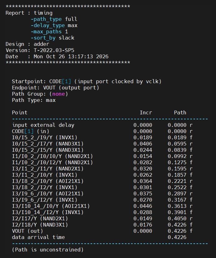
The adder went from 645 ps to 422.6 ps, a 34% reduction:
- Downsized COUT's output inverter from INVX4 to INVX1, since the large device was driving a small load and only added delay (645 ps to 510 ps).
- Restructured bit 0's generate into a single NAND-NAND majority function using a new dedicated cell that computes the effective carry-in directly from the opcode and CIN, in parallel with the slower B-select path (493 ps).
- Buffered the heavily loaded low-order signals g<0> and c<2> with double inverters so their fanout no longer loaded the critical path (467 ps).
- Rewrote overflow to derive directly from c<15>, g<15>, and p<15>, removing one gate of depth from the latest-arriving signal (447 ps).
- Reordered pins on the critical path so the latest-arriving input lands on the fastest physical pin (pin B on a NAND2, pin C on a NAND3), which are measurably faster than pin A because of transistor stacking order (about 426 ps).
- Added a final buffer on c<3> to relieve its fanout (422.6 ps).
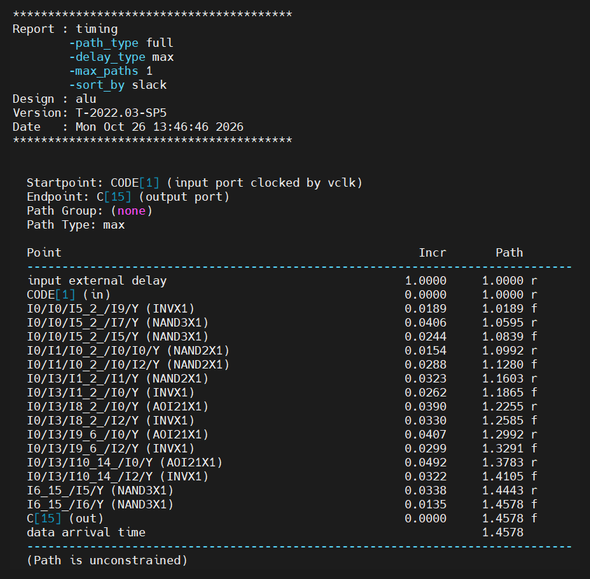
The ALU went from 549 ps to 457.8 ps, a 17% reduction. Most adder optimizations carried over because the ALU shares the adder core. After that, the critical path moved from block to block. The shifter became the bottleneck because one rotate-control signal drove both the left and right rotate stages, so I split it into two independently buffered signals. The comparator became the next bottleneck, so I restructured its operation select around AOI21 gates and moved its result onto the fastest input pin of the final output NAND3. The end state has the adder (457.8 ps), shifter (448.5 ps), and comparator (445 ps) within about 13 ps of each other, so no single datapath dominates and further speedup would require restructuring several units at once.
Place and Route in Innovus
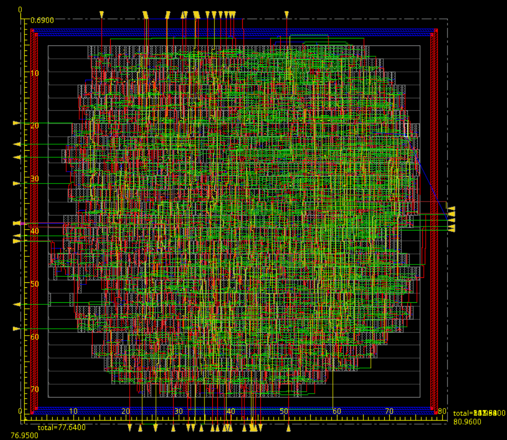
With the netlist functionally verified and timing optimized, I took the roughly 1,800-cell ALU through a full automated flow in Cadence Innovus. The block is purely combinational, so no clock tree was needed. I imported the netlist and the 45nm technology LEF, set the core utilization, aspect ratio, and row spacing in the floorplan, added a core power ring on metal1 and metal2 for VDD and VSS, ran automated placement, and then global and detailed routing across all metal layers.
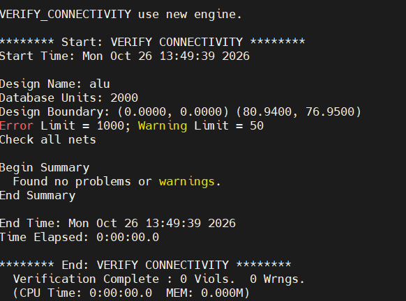
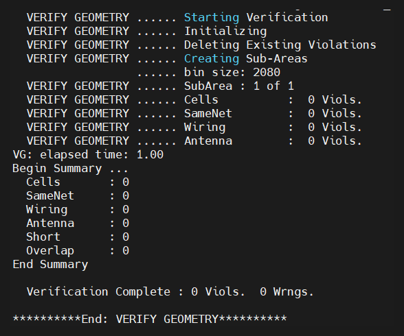
I then ran verifyGeometry and verifyConnectivity as physical sign-off. Both finished with 0 violations and 0 warnings across cells, same-net, wiring, antenna, short, and overlap checks, and all 1,817 cell instances were placed and connected, matching the source netlist one for one. The final die measures 80.96 µm by 76.95 µm, about 6,230 µm².
Physical Verification
The Innovus verifyConnectivity and verifyGeometry logs for the final routed design both report 0 violations and 0 warnings.
Post-Layout Timing
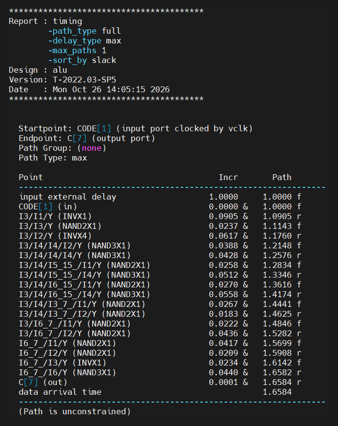
To see what the real layout does to timing, I extracted RC parasitics from the routed geometry into a SPEF file (1,853 of 1,855 nets annotated) and re-ran PrimeTime using actual wire resistance and capacitance in place of wire-load estimates. Data arrival moved from 1.4578 ns before layout to 1.6584 ns after, about 200 ps slower, which is entirely real interconnect RC that a wire-load model cannot predict. Both figures include the 1 ns input delay constraint, so the logic delay went from 457.8 ps to 658.4 ps, roughly 44% slower. The critical path also moved from C[15] to C[7], with the shifter becoming dominant after layout. A design that looks fast on paper can slow down substantially once real wiring is accounted for, which is why post-layout sign-off matters, and the size of the gap shows how wire-dominated the design is at this node.
Results
- Adder critical path: 422.6 ps, down from 645 ps (34% reduction).
- ALU pre-layout delay: 457.8 ps, down from 549 ps (17% reduction).
- ALU post-layout delay: 658.4 ps of logic (1.6584 ns including the 1 ns input delay), using extracted parasitics.
- Gate count: 562 for the adder, 1,817 for the ALU, using only NAND2X1, NAND3X1, AOI21X1, INVX1, and INVX4.
- Verification: 0 errors across 20,000+ random adder vectors, 22,000+ random ALU vectors, and all official vectors.
- Physical verification: 0 DRC violations and 0 connectivity violations.
- Die area: 80.96 µm by 76.95 µm, about 6,230 µm².