4-Bit SRAM Memory Cell
45nm FreePDK, Cadence Virtuoso and Calibre, HSPICE
Introduction
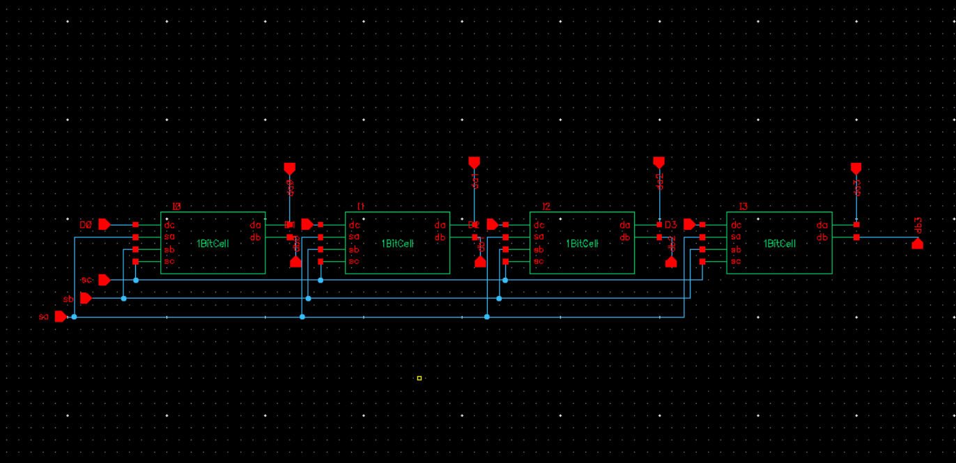
I designed, laid out, and verified a 4-bit latch-based SRAM memory cell in a 45nm process, taking it from a transistor-level schematic through a hand-drawn custom layout, physical verification, parasitic extraction, and post-layout simulation. Each bit is a latch with one write port and two independent read ports, and the four bits share their write and read control lines, so the cell is a small building block that could be tiled into a larger memory array.
The layout was limited to three metal layers, with a VDD rail down the right side and a GND rail down the left, and it had to pass DRC and LVS and still read back the data that was written once real parasitics were included.
Circuit Architecture
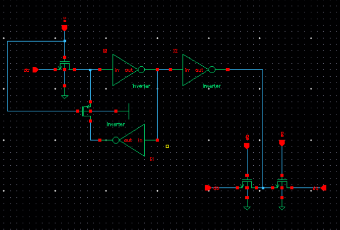
Each bit stores its value in two inverters connected back to back. A pMOS pass transistor in the feedback path is on while the write control sc is 0, so the stored value circulates through the loop and is held. When sc goes to 1, the pMOS turns off and breaks the loop, and an nMOS pass transistor connects the data input dc to the storage node, forcing that value into the latch. A third inverter acts as an inverting buffer so the correct logic value appears at the read ports, and two more nMOS pass transistors, controlled by sa and sb, connect that buffer to the output lines da and db. That gives each bit one write port and two read ports.
The devices were sized with 170 nm wide nMOS and 340 nm wide pMOS transistors, all with a 60 nm gate length. The transistor budget for one bit is:
- Three inverters (6 transistors): the two cross-coupled storage inverters and the read buffer.
- One write pass nMOS (1 transistor), gated by sc.
- One feedback pass pMOS (1 transistor), on when sc is 0 to hold the stored value.
- Two read pass nMOS (2 transistors), gated by sa and sb.
That makes 10 transistors per bit (6 nMOS and 4 pMOS), so the 4-bit cell has 40 transistors (24 nMOS and 16 pMOS). Each bit has its own data input and its own da and db outputs, and all four bits share sa, sb, and sc, so the 4-bit cell has 4 data inputs, 8 data outputs, 3 control inputs, VDD, and GND, which is 17 pins in total.
Custom Layout
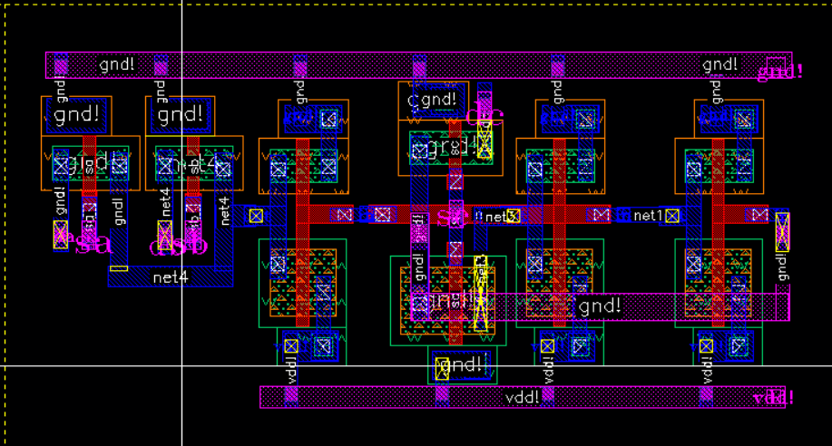
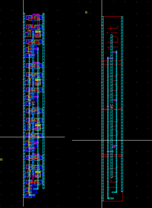
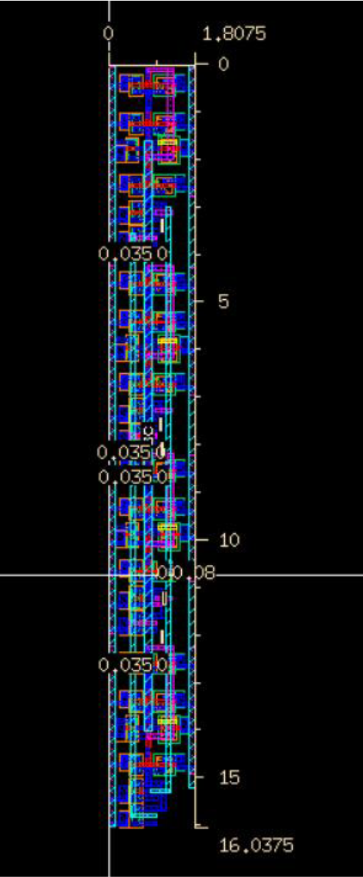
I drew the layout by hand instead of building it from the standard inverter cell. Reusing a pre-made cell is faster, but a standard-cell layout comes out larger than a custom one. Drawing every transistor directly let me place each device where the circuit needed it. The final cell is four identical bit slices stacked vertically into a tall, narrow strip, with the shared control lines running along it, the VDD rail on the right edge, and the GND rail on the left.
Three techniques did most of the work of keeping the area down:
- Custom layout instead of standard cells, so no device or spacing exists only to make a reusable cell.
- Shared taps and wells with transistors aligned in rows, so one well contact serves several devices instead of every transistor carrying its own.
- Using every allowed metal layer (M1 and M2 in the 1-bit cell, with M3 added for the 4-bit cell), so routing goes over the devices instead of widening the cell.
Area
I measured the final layout with rulers in Virtuoso. It is 16.0375 µm tall and 1.8075 µm wide, for a total area of 28.9878 µm². That works out to about 7.25 µm² per bit, or about 0.72 µm² per transistor.
Physical Verification
The final layout passes DRC and passes LVS, so the layout matches the schematic transistor for transistor. Parasitic extraction ran clean and produced the extracted netlist used for the post-layout simulation.
Post-Layout Verification
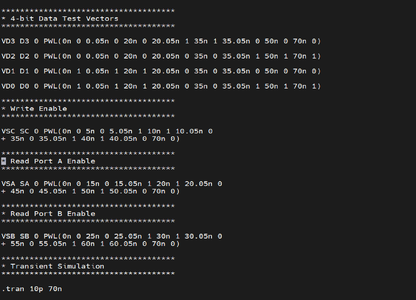
I verified the cell by simulating the extracted layout in HSPICE, so the real wire resistance and capacitance of the layout are included. The test bench uses the 45nm transistor models at 1.0 V and 25 degrees C, drives the four data inputs and three control lines with piecewise-linear sources with 50 ps edges, and runs a 70 ns transient.
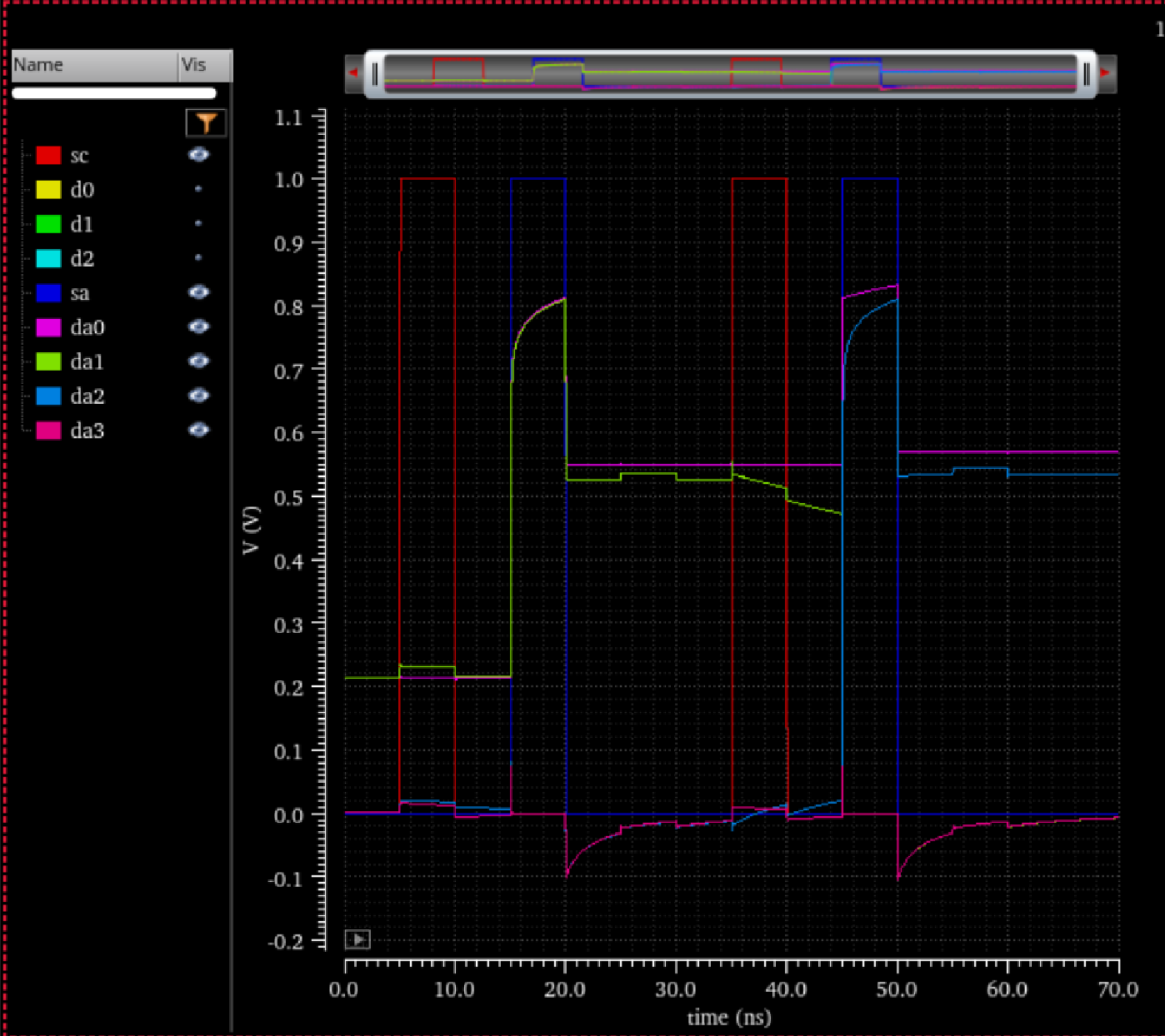
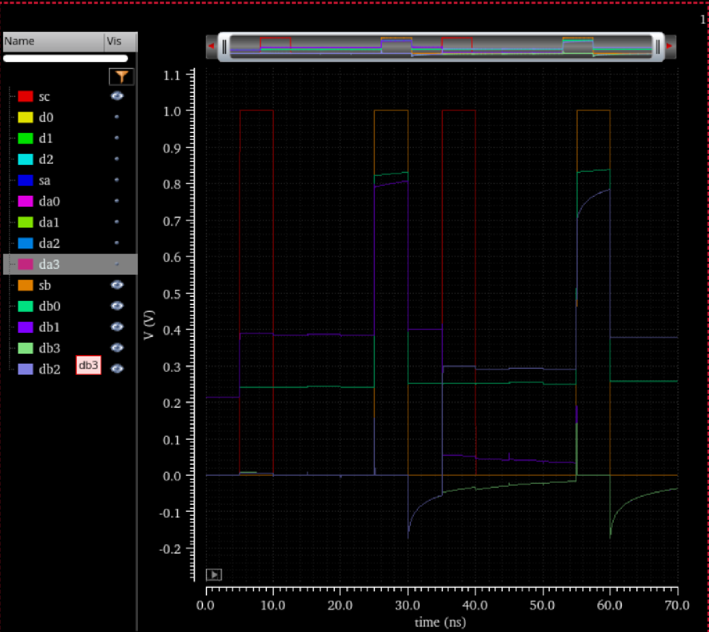
The test sequence writes 0011 (sc high from 5 to 10 ns) and reads it back on port A (15 to 20 ns). It then changes the data inputs to 1000 while sc is low and reads port B (25 to 30 ns), which checks that the cell holds its value and ignores the data lines when it is not being written. Finally it writes 0101 (35 to 40 ns) and reads that back on port A (45 to 50 ns) and port B (55 to 60 ns).
Simulation Results
The outputs match the stored data on both ports in both reads. In the first port A read, da0 and da1 go high while da2 and da3 stay low, reading back 0011. In the second, da0 and da2 go high, reading back 0101. Port B shows the same pattern on db0 through db3. High read outputs settle near 0.8 V, which is expected for outputs driven through nMOS pass transistors, and port B returned 0011 correctly after the data inputs had changed, so the cell held its data while it was not being written.
Results
- Transistors: 10 per bit, 40 for the 4-bit cell (24 nMOS and 16 pMOS).
- Ports: 1 write port and 2 read ports per bit, with 4 data inputs, 8 data outputs, and 3 shared controls (17 pins including VDD and GND).
- Area: 28.9878 µm² (16.0375 µm by 1.8075 µm), about 7.25 µm² per bit.
- Metal layers: M1 through M3 only.
- Physical verification: DRC, LVS, and parasitic extraction all clean.
- Functional verification: post-layout HSPICE confirms writing and reading back 0011 and 0101 on both read ports.